Home Matrix Multiplication and Efficiency of Multimodal LLM with Gemini-II
Associative computing applies operations to data based on content rather than address, enabling massive parallelism across memory arrays. Compute‑in‑memory (CIM) extends this concept by performing computation directly in or on memory structures, minimizing data movement.
This whitepaper discusses how GSI Technology’s Associative Processing Unit (APU) performs matrix multiplication and then shows why it is a superior solution to achieve TTFT in multimodal LLM with Text and Video inputs that are useful for edge physical AI awareness.
Figure 1 shows a partial representation of the bit-processor structure used in GSI Technology’s CIM chip, Gemini-II. This implements a highly optimal RISC Boolean processor due to its ability to read multiple memory bit cells onto a single memory line. Multiple word lines could turn on to generate Boolean functions on the bit line that would create a collision and garbage on a regular memory and is not an allowed operation on general purpose memory. The computation core array and memory cell are expounded upon in greater detail in patent US10877731B1.
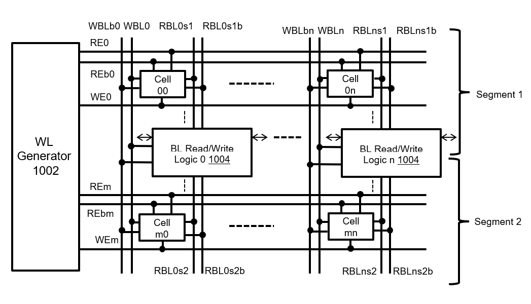
Figure 1: Bit-Processor Structure for Gemini-II
Figure 2 shows an illustration of a dual port SRAM cell capable of performing a XOR Boolean operation and a multi-bit full adder using the XOR capability. These are expounded upon in greater detail in patent US11604850B2, particularly their use in creating a hardware in-memory full adder.
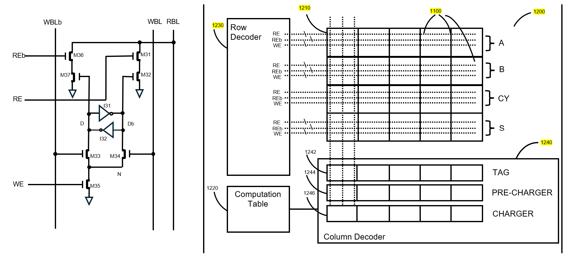
Figure 2: Dual Port SRAM Cell
A key property of bit‑line CIM is bit‑slice flexibility:
GSI emphasizes 1‑bit granularity and user‑defined bit frameworks, enabling dynamic precision tradeoffs between accuracy, performance, and energy. To provide an example of the flexibility though, it is noted that a customer in the medical research industry used this architecture to implement a 2048-bit “word” for use in molecular representation.
Let’s start with multiplication.
Any multi‑bit multiplication can be decomposed into bitwise partial products:
Thus, multiplication reduces to:
Digital CIM arrays are well‑suited to step (1) at massive parallelism and can implement steps (2)–(3) using in‑memory adders.
A multiply‑accumulate (MAC) operation computes:
This definition is implementation‑independent. A MAC may be:
Let’s look at as an n-bit unsigned integer, as an m-bit unsigned integer, and acc as a k-bit unsigned integer accumulator.
Each Bit-line Processor (BP) in the Gemini-II APU contains local memory and a 1-bit full adder. The full adder can perform one full-adder operation per cycle.
Multiplying an n-bit number by an m-bit number requires n × m full-adder operations. Adding the result to the k-bit accumulator acc requires k additional full-adder operations. Therefore, a single MAC requires n × m + k full-adder operations when all values are stored in BP memory.
All arithmetic described here assumes unsigned integers.
The Gemini-II APU contains 1 million (2²⁰) Bit-line Processors. Each BP performs one full-adder operation per cycle, with a cycle time of 0.83 nanoseconds (1.2GHz clock).
We can also do a sequence of MAC operations.
In matrix multiplication:
tiles of matrices A and B are loaded into the APU memory. Each BP computes one output element of matrix C as a dot product, which consists of a sequence of MAC operations.
For each MAC in the sequence, a new value of A is broadcast to the Bit-line Processors.
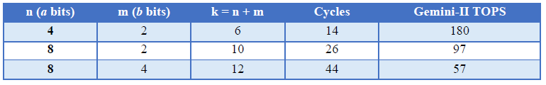
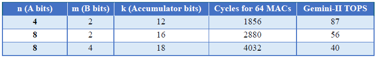
When multiple MAC operations are performed, the accumulator must be wider to avoid overflow. For a sequence of 64 MAC operations, the accumulator size is k = n + m + 6 bits.
Broadcasting the value of A to the Bit-line Processors takes n + 5 cycles per MAC.
The Jetson Orin series uses Ampere GPU with varying SMs, CUDA cores, Tensor Cores, and shared memory/L1, L2 and DRAM. The Jetson Thor uses a Blackwell GPU with ~20 SMs, 2560 CUDA cores, 96 Tensor Cores, ~228 KB shared memory per SM, and ~32 MB L2.
Tensor cores operate on matrix fragments in registers, which must be loaded from shared memory. General matrix-to-matrix multiplication, GEMM, kernels rely on tiling into SMEM, asynchronously copies from generalized memory management to shared memory (GMEMßà SMEM), and reuse. For large GEMMs, performance often becomes memory-/data-movement-bound, not Tensor Core FLOP-bound.
Thus, Tensor Cores raise compute throughput, but do not change the requirements to tile A/B and repeatedly move tiles between DRAM, L2, SMEM, and registers when matrices are larger than SMEM/L2.
Consider a single large GEMM on the TTFT critical path (e.g., in Gemma‑3 12B + SigLIP):
Matrices:
Assuming float32 (4 bytes):
One token (row of A) = 4096 × 4 = 16 KB.
In Gemini‑II compute‑in‑memory capacity ≈ 96 MB.
Max rows of A fitting on-chip:
For a 1024‑token context:
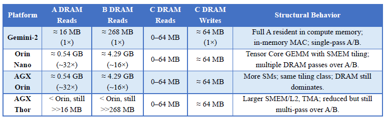
Execution on Gemini‑II:
TTFT is dominated by one pass over A/B and one C write.
On Orin (Ampere):
Using typical Tensor Core GEMM tiling (per NVIDIA docs):
Each C tile:
Effective DRAM read factors for large GEMMs remain approximately:
On Thor:
Yet, as CUTLASS Blackwell docs and microbenchmarks show:
Thor lowers effective DRAM reads per element vs Orin Nano/AGX but does not reach Gemini-II’s ~1× read.
Transformer inference relies heavily on matrix multiplication in:
This paper showed efficiencies available in the GSI CIM Associative Processing Unit when implementing arithmetic logical operations. The combination of dynamic frameworks, and efficient data sequencing available through flexible bit-slice arithmetic logic implementation provides multi-modal vision, text, and sensor LLM processing at latencies that make awareness for edge physical AI. For example, running full Gemma-3, 12B with SigLip allows a streaming analysis whereby only the first tokens are analyzed for environmental awareness. This was shown to have reduced external DRAM transfers, which are the limiting factor for LLMs. This was shown on a recent press release7 on a Gemini-II processor such a workload results in 3 second response times (e.g., person performing suspicious activity, city infrastructure damaged, etc.) at 30 watts, which is usable for edge awareness applications such as smart city pole cameras, autonomous mobile robots, or drones.
References (Complete)
https://ir.gsitechnology.com/news-releases/news-release-details/gsi-technology-reports-3-second-time-first-token-edge-multimodal